Vigie 1.0
Technical documentation
Architecture, board, measurement, firmware and network of Vigie 1.0 — work in progress.
Vigie is a single board that measures the energy of a sailboat or a 12 V battery pack, keeps watch all year and reports. It replaces the “ESP32 devkit + INA226 module + LM2596 converter” stack with an 86 × 54 mm four-layer board, and sits upstream of the main switch — the one module that stays alive through the winter: its converters draw 22 µA per stage, and the whole board stays below a milliamp.
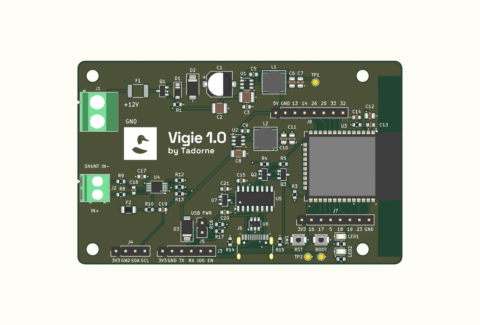
Overview
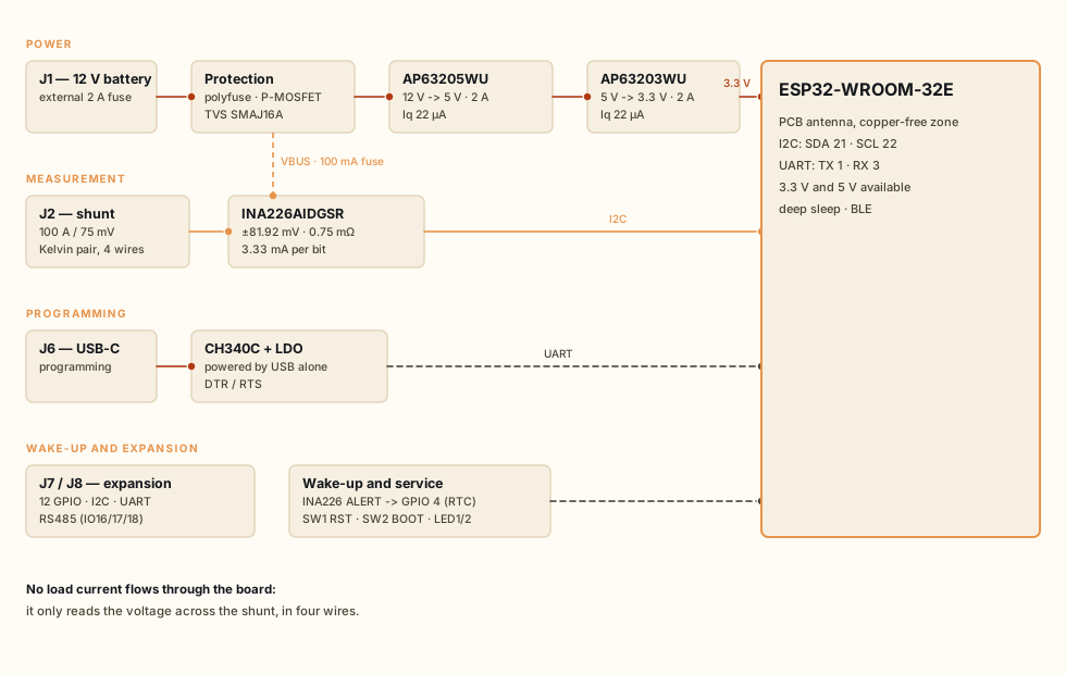
One point of truth: all current aboard flows through a 100 A / 75 mV shunt in the negative bus, and the board only reads the voltage across it, in four wires. No load current flows through the board.
| Characteristic | Value |
|---|---|
| Dimensions | 86 × 54 mm, R2 corners, four M3 holes |
| Layers | 4: signal / ground plane / +3.3 V plane / signal |
| Microcontroller | ESP32-WROOM-32E, PCB antenna on the right flank, copper-free zone on all four layers |
| Measurement | INA226AIDGSR, external 100 A / 75 mV shunt, four-wire Kelvin connection |
| Power | 12 V → 5 V → 3.3 V, 2 A per stage, 22 µA quiescent current per stage |
| Protection | polyfuse, reverse-polarity P-MOSFET, SMAJ16A TVS, 100 mA fuse on VBUS |
| Programming | CH340C + USB-C, automatic DTR/RTS reset |
| Expansion | two 1×8 headers: 12 GPIO, +3.3 V, +5 V, I2C, UART, reserved RS485 |
| Footprints | 69 footprints and 4 holes, 54 nets |
The board
Power
Two switching converters from the same family share the chain: AP63205WU for 12 V → 5 V and AP63203WU for 5 V → 3.3 V, 2 A each at 1.1 MHz. The hard point of an always-on node is their quiescent current: 22 µA per stage, where an LM2596 draws 5 to 10 mA continuously, about 3.5 Ah a month taken for nothing.
The input is protected by a polyfuse, a reverse-polarity P-MOSFET (45 mΩ, with its gate zener — mandatory, since the battery reaches 14.4 V while charging) and an SMAJ16A TVS. On the bench, jumper J5 powers the board from USB; it is open by default so the 5 V cannot climb back to the battery terminal. The CH340C is powered by an LDO taken from USB VBUS alone: unplugged, it draws nothing.
Measurement
The INA226 works across a 0.75 mΩ shunt in the negative bus: 75 mV of common
mode instead of 12 V, and VBUS reads the battery voltage directly. Its range is
fixed at ±81.92 mV — the ADCRANGE bit does not exist on this part, unlike
the INA228 — which gives, with the native 2.5 µV step, a resolution of
3.33 mA. One hundred amps use 91.6 % of full scale.
Gain, zero and current sign are set in software (i_gain, i_offset_mA,
i_invert): a J2 wired the wrong way round is corrected without taking the
board apart. Amp-hour counting is software too, since the INA226 has no charge
accumulator. Finally, ALERT arrives on GPIO 4, an RTC pin: it can wake the
ESP32 from deep sleep.
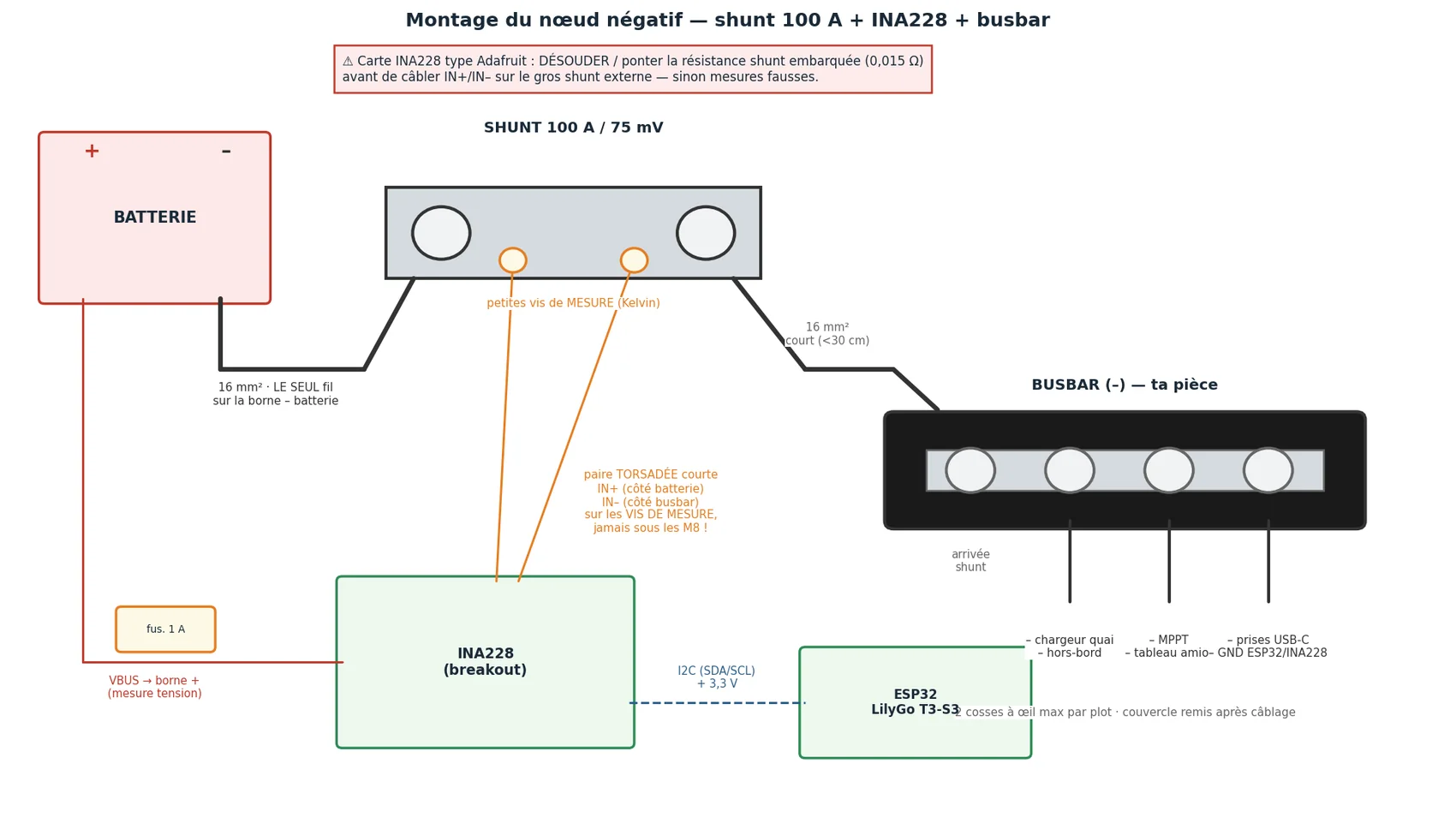
The precaution is not theoretical: at 100 A, 20 cm of 16 mm² cable is already 23 mV, close to a third of the measurement range.
Routing and placement
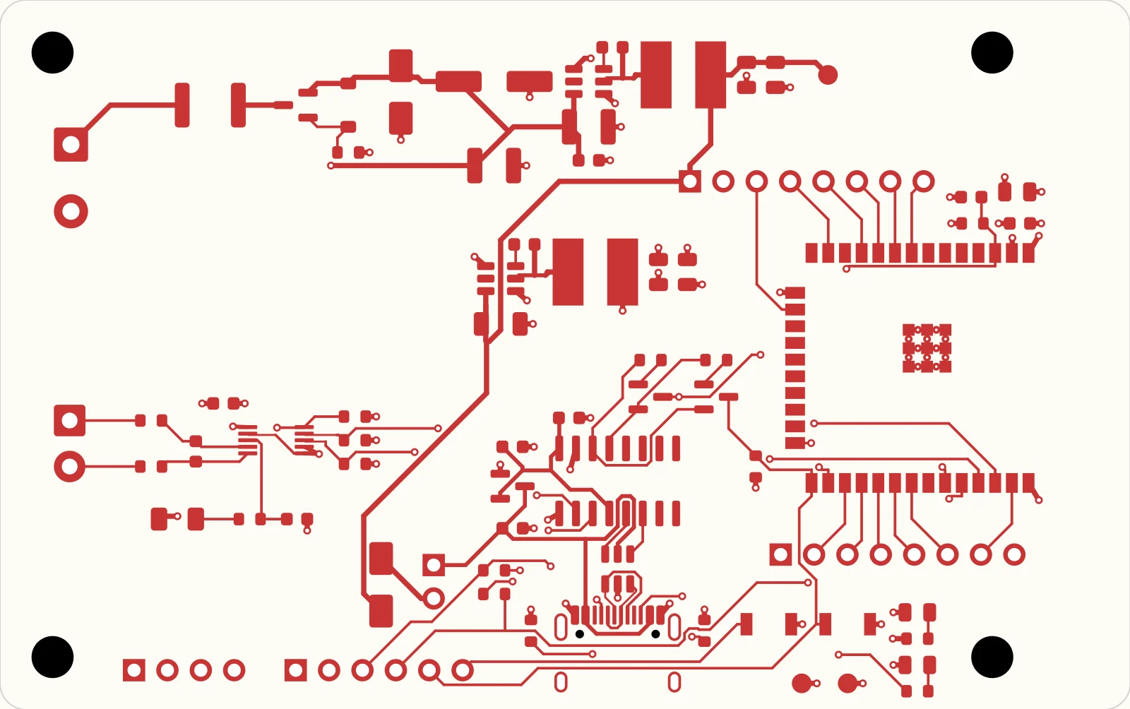
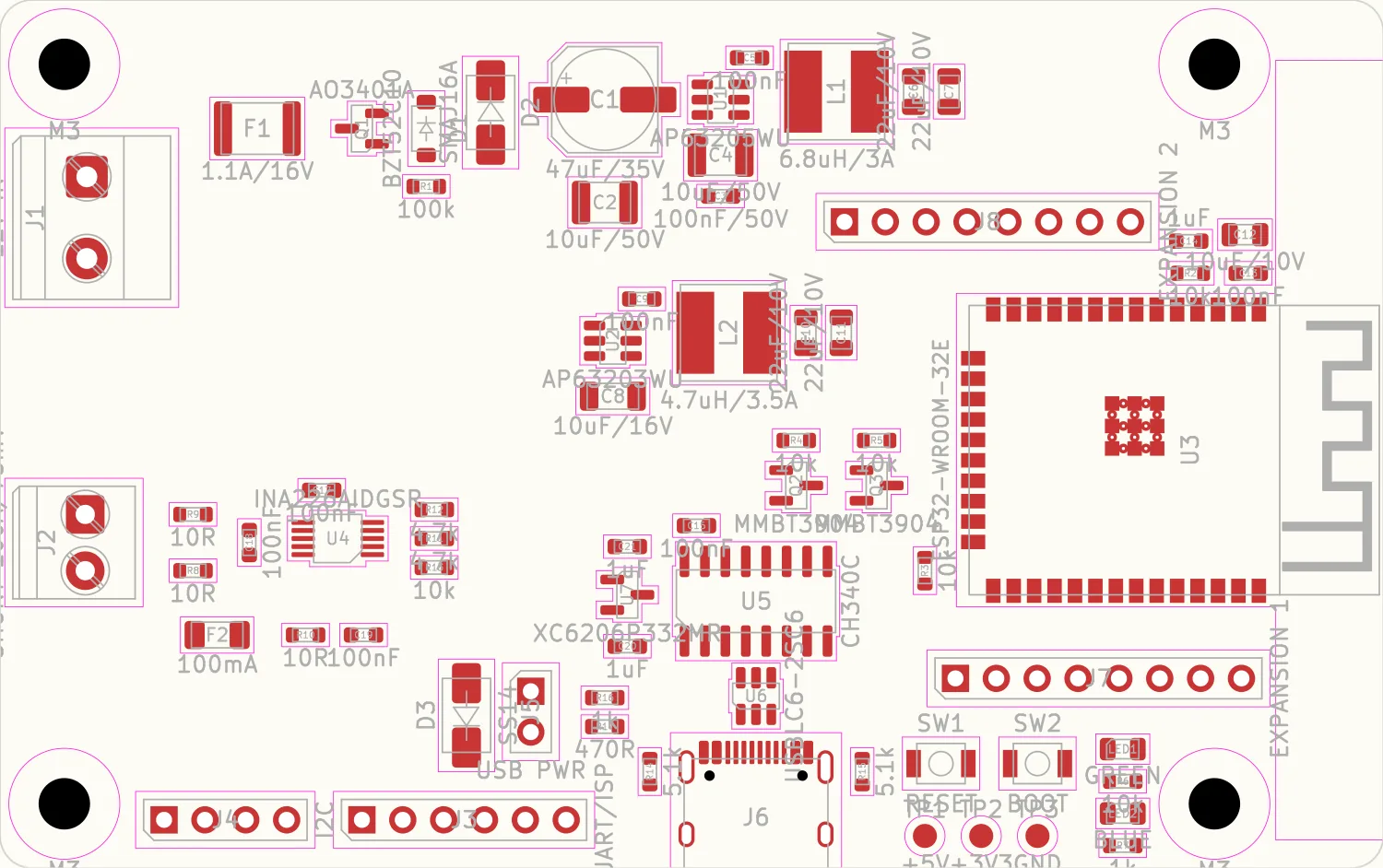
The two inner layers are solid planes with no tracks at all: In1 for ground, In2 for +3.3 V. Every SMD ground and +3.3 V pad drops to its plane through its own via, placed and locked before routing. Signal routing fits on the two outer layers.
Connectors
| Ref. | Role | Pinout |
|---|---|---|
| J1 | 12 V input (5.08 mm terminal block) | 1 = +12 V battery (external 2 A fuse) · 2 = GND, load side of the negative bus |
| J2 | Shunt (3.5 mm terminal block) | 1 = IN− · 2 = IN+ — sign to be confirmed at bring-up |
| J3 | UART / ISP | 3V3 · GND · TX · RX · IO0 · EN |
| J4 | I2C | 3V3 · GND · SDA · SCL |
| J5 | USB PWR jumper | close to power from USB, without the battery only |
| J6 | USB-C | programming |
| J7 | Expansion 1 | 3V3 · IO16 · IO17 · IO5 · IO18 · IO19 · IO23 · GND |
| J8 | Expansion 2 | 5V · GND · IO13 · IO14 · IO26 · IO25 · IO33 · IO32 |
I2C is on SDA 21 / SCL 22, the status LED on GPIO 2, the BOOT button on GPIO 0, the console on TX 1 / RX 3. GPIO 16, 17 and 18 are grouped on J7 for the MPPT’s future RS485. The strapping pins 12 and 15, like GPIO 34 to 39, are not brought out.
Firmware
The firmware runs on PlatformIO, with a pinned pioarduino platform
(Arduino-ESP32 3.3.11 / ESP-IDF 5.5) and no external library. It is published as
version 1.0.0 under the GPL-3.0 licence, in the
firmware/ folder of
the repository. It also runs on a bare ESP32
devkit: a battery simulator stands in for the missing INA226, and every
simulated measurement carries the SIM flag all the way into the log and onto
the air.
The cycle is deep sleep broken by short wake-ups:
| Task | Default period | Cost |
|---|---|---|
| Measurement | 5 min | 110 ms awake |
| Recording | 5 min | average, minimum and maximum of the period |
| Brief BLE advertisement | at every measurement | about 0.4 s awake, estimated |
| Radio push | 15 min | 1.8 s awake, of which 1.1 s of BLE advertising |
| Wintering | push every 6 h | survival mode |
Measurement averages 1024 INA226 conversions, a 9.6 s sliding window that keeps averaging while the ESP32 sleeps. State of charge is coulometric counting: trapezoids between measurements, 0.90 charge efficiency, Peukert exponent 1.25 in discharge beyond C/20. It resynchronises to 100 % when the voltage holds above the threshold with a low tail current, and re-anchors on the open-circuit voltage table after four hours at rest.
The log lives in a raw 896 KB partition, with no file system: 32-byte records
protected by a CRC. At the default cadence the ring keeps about 95 days of
samples and 2.5 years of daily summaries. The board has no backed-up clock:
time arrives from the admin page, from the gateway or from the console, and a
time_sync record makes it possible to date what came before.
Battery protection is a staircase, and a degradation needs two consecutive evaluations — an engine start does not cut the node:
| Voltage | State | Effect |
|---|---|---|
| 12.2 V and above | nominal | |
| below 12.2 V | throttled | push halved |
| below 11.9 V | survival | push every 6 h, no catch-up |
| below 11.5 V | cutoff | final alert, then radio silence; the INA226 wakes the node once the voltage is back above 12.6 V |
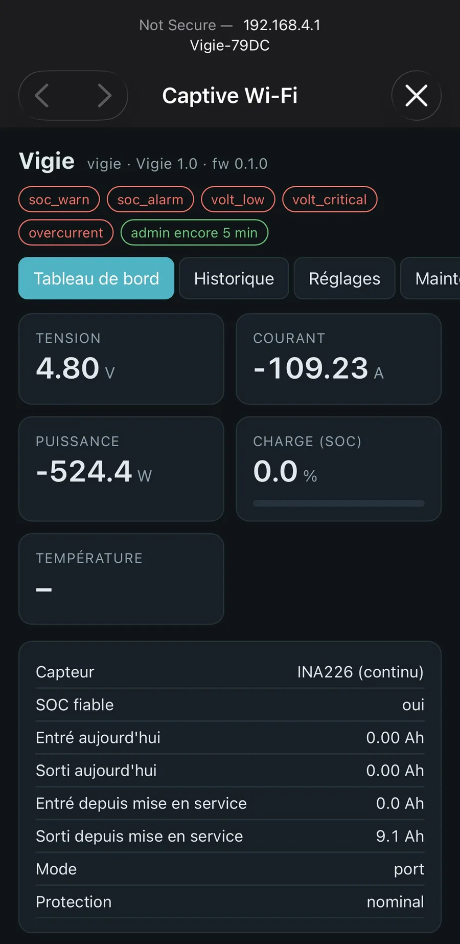
Administration is an access point, Vigie-XXXX (WPA2, captive portal), opened
on cold start or by holding BOOT: dashboard, 6 h to 30 day history with CSV
exports, settings, SOC reset, OTA update and log erase. The serial console
offers the same functions.
The enclosure and the TPU sole
The node sits in an off-the-shelf IP67 sealed enclosure: the enclosure provides the sealing, and a TPU 95A sole takes care of the mechanical fit. It lines the bottom of the enclosure, carries the shunt in a cradle whose lips close over the blocks, and houses the board on four posts. A pad, glued under the lid, presses on the cradle with 1.5 mm of crush: the shunt is clamped between the floor and the lid, with no play.
The sole prints at 25 % gyroid, the pad at 100 %; the cradle comes out solid
thanks to an infill modifier. The OpenSCAD source, the STL files and the Cura
profiles are in the
mecanique/ folder.
Several dimensions of this enclosure are
still to be taken from the real part.
Network and application
The node pushes its measurements in two complementary ways. On the local
network, TsubameBus: encrypted ESP-NOW frames, a 12-byte header and a CBOR
body, with HELLO, ENERGY, ALERT and LOG_BATCH. A receiver acknowledges
the last record it got, so a module absent for a week recovers the whole week
when it returns. Towards phones, a BTHome v2
advertisement over Bluetooth LE, readable as-is by Home Assistant or nRF
Connect, with optional AES-CCM encryption.
A Signal K implementation is planned.
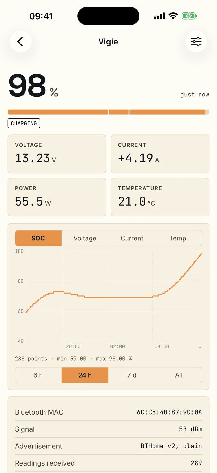
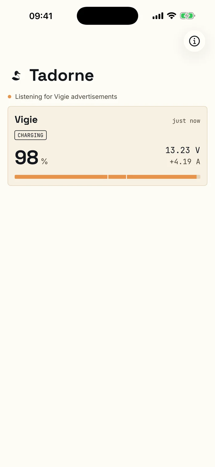
| What Vigie broadcasts | Received by an iPhone | Content |
|---|---|---|
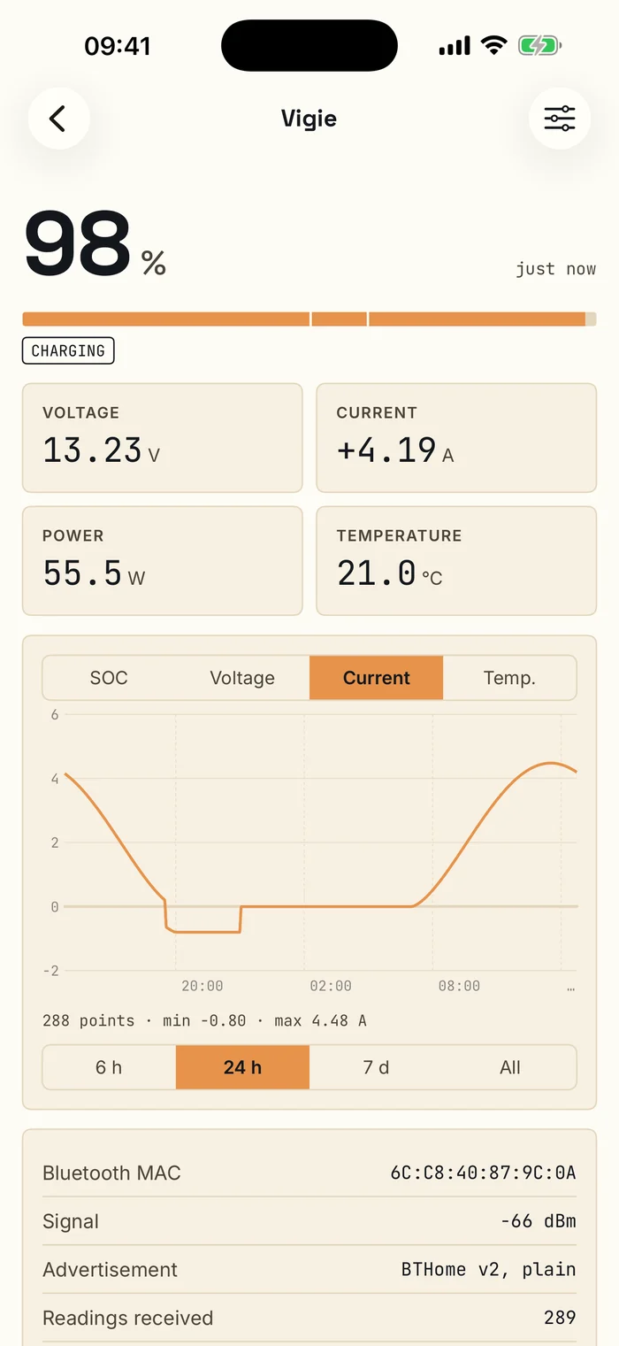
| BLE BTHome v2 advertisement | yes | state of charge, voltage, current, power, temperature |
| Scan response (manufacturer block) | yes | Bluetooth MAC, status flags, active alerts |
| ESP-NOW frames | no | iOS gives no access to raw Wi-Fi frames |
The Tadorne iPhone app listens passively: no connection, no pairing, nothing is transmitted. It keeps the history of what it caught, with the app open; the full log stays in the node’s flash.
This revision of the board carries neither LoRa nor LTE: it is the measurement post, not the Internet gateway. The radio arbitration remains open, and the gateway will join the network without modifying the board.
State and open points
| Point | State |
|---|---|
| Real quiescent current | to be measured at bring-up — it is what sets the winter autonomy |
| Current sign at the shunt | to be confirmed at first wiring |
| Antenna in a closed locker, in the bilge | open point; the ESP32-WROOM-32UE variant, with a u.FL remote antenna, fits the same footprint |
| RS485 for the EPEver MPPT | not fitted; external MAX3485 module on J7 |
| Firmware | published as 1.0.0 (GPL-3.0) |
| Enclosure | TPU sole and pad published; enclosure dimensions to be measured |
| Bill of materials and calibration procedure | to come |
The bench validated the build of all three environments, the sleep cycle, the log and its recovery after reset, the 100 % resynchronisation and the low-voltage cutoff. Real ESP-NOW frame reception, BLE reception and everything touching the real INA226 remain to be verified on the board.